

Micro-electro-mechanical systems (MEMS), also known as microsystems, are a technological framework that integrates mechanical structures and electronic circuits at the microscale, and represent one of the key enabling technologies in the practical implementation of the Internet of Things. We will now discuss the assembly and composition of micro-electro-mechanical systems, their technical foundations, manufacturing processes and future development trends.
One type of technological system, known as a microsystem—specifically a micro-electro-mechanical system, or MEMS (the ‘micro-’ in MEMS)—achieves the integration of mechanical structures and electronic circuits at the microscale, and is one of the core enabling technologies in the implementation of the Internet of Things.
Devices containing accelerometers, gyroscopes, pressure sensors, micro-mirrors, inkjet printheads, microphones and loudspeakers, amongst others, are typical examples of MEMS devices. During the manufacture and assembly of such devices, semiconductor processes are predominantly employed. At the heart of these devices lies a chip-scale integrated MEMS chip, which integrates micromechanical structures with electronic circuits on a single substrate, thereby forming a fully functional microdevice.
At present, MEMS—which are regarded as key electronic components—have become widely integrated into a range of sectors, including domestic appliances, automotive electronics, Internet of Things (IoT) devices, communications equipment and medical devices.
MEMS and integrated circuits (ICs) share many commonalities in terms of manufacturing processes and miniaturisation technology; however, the differences between the two are quite significant in terms of their functional roles, operating principles and application scenarios.
An integrated circuit, comprising purely electronic components such as transistors, capacitors and resistors, serves primarily to process, control and perform logical operations on electrical signals, as well as to store data; it is the “information processing core” of electronic devices.
As MEMS treats physical motion and the measurement of physical quantities as its core functions, it consists of sensors—that is, signal-detection units—and actuators—that is, drive units—with a focus on achieving the conversion of “physical quantities to electrical signals” or the driving of mechanical movements. In terms of structure and form, the diverse application scenarios of MEMS result in significant variations in their appearance, internal structure and dimensions; everything from sensor chips at the micrometre scale to integrated micro-actuators falls within the scope of MEMS. In addition to the sensors and acoustic devices mentioned earlier, typical applications also include functional components such as micro-valves and optical switches.
A vivid analogy can help to understand the roles of the two: if we compare integrated circuits, which specialise in information processing and storage, to the human brain, then MEMS—which combine mechanical motion and sensing functions and perform various physical actions—are akin to the human body’s motor system and sensory organs. The former are responsible for information processing and memory, whilst the latter is responsible for environmental perception and the execution of actions; together, they work in concert to support the comprehensive functionality of modern electronic devices.
Definition and Core Components of Micro-Electro-Mechanical Systems
In micro-electro-mechanical systems (MEMS), the key physical dimensions range from well under 1 micrometre to as large as several millimetres. The key criterion for determining whether a system is a MEMS lies in whether its substrate contains at least some components with mechanical functions, regardless of whether these components are capable of movement. The types of devices it encompasses are extremely diverse, ranging from simple structures with no mechanically moving components to complex mechatronic systems that integrate microelectronic technology with micromechanical structures on a single silicon substrate.
A key component of micro-electro-mechanical systems (MEMS) is the microsensor, which is a type of “transducer” capable of converting one form of energy into another. MEMS also comprise microactuators, which are likewise “transducers” capable of converting one form of energy into another.
Microsensors are capable of sensing their environment; they can convert physical or chemical signals—such as temperature, pressure, inertial forces, chemical substances, magnetic fields and radiation—into electrical or optical signals. Over the past few decades, researchers have developed microsensors covering almost all sensing modalities, with many outperforming their macroscopic counterparts. For example, micro-electromechanical system (MEMS) pressure sensors demonstrate superior performance in terms of accuracy and response speed.
Drawing on the mass production techniques used in the integrated circuit (IC) industry, it has significantly reduced the cost per device whilst ensuring that performance is maintained. This has enabled the commercialisation of silicon-based discrete microsensors, and the associated market continues to grow.
Micro-actuators, as the actuating components within micro-electro-mechanical systems (MEMS), are tiny in size yet capable of exerting an impact on a macroscopic scale. A wide variety of micro-actuators have now been developed, including micro-valves that control the flow of gases and liquids, as well as optical switches and mirrors that alter the direction of light beams, as well as independently controlled micromirror arrays for display purposes, micro-resonators suitable for a wide range of operating conditions, micro-pumps capable of generating positive fluid pressure, and micro-flaps for regulating airflow over aircraft wings, amongst others.
Researchers fitted small microactuators to the leading edge of the aircraft’s wing and, using only these miniature devices, achieved manoeuvrability control. Whilst flying at high speed, the aircraft was able to perform a 180-degree turn with a turning radius of nearly one wing radius.
It is only when microsensors, microactuators and integrated circuits are integrated onto the same substrate that the full potential of micro-electro-mechanical systems (MEMS) can be realised. Sensors are responsible for gathering environmental information; electronic devices process this information and make decisions; and actuators carry out operations based on these decisions, thereby altering the state of the environment. It is precisely this collaborative model that makes MEMS a vital component of the Internet of Things (IoT). Like “eyes, ears and nose”, they continuously collect, store, process and exchange information, working in tandem with other networked devices to perceive and control the environment.
Core characteristics of micro-electromechanical systems (MEMS) technology
Micro-electro-mechanical systems (MEMS) technology possesses its own distinctive characteristics, which enable it to play a crucial role in many fields.
It is manufactured using integrated circuit-style processes, enabling multiple functions to be integrated onto a single microchip. Microsensors can be integrated, microactuators can be integrated, and microstructures can also be integrated with microelectronics; this not only enhances the functional density of the product but also provides vital support for the realisation of the Internet of Things.
From a cost perspective, it draws on the mass production processes used in the integrated circuit sector, although the production equipment and the initial cost per wafer are by no means inexpensive, the costs can be spread across a large number of chips through mass production, thereby significantly reducing the cost of individual devices or microchips within complex micro-electromechanical systems, It is precisely this cost-effectiveness that enables MEMS to be deployed on a large scale, whilst also making maintenance and replacement more cost-effective.
Thanks to integrated circuit manufacturing technology and the mechanical advantages of silicon and various other thin-film materials, the combination of these two factors has significantly enhanced the stability and durability of micro-electromechanical products; this is one of the major advantages of micro-electromechanical systems. As the core material, silicon has a yield strength close to that of stainless steel and ranks among the highest in terms of strength-to-weight ratio among engineering materials, thereby laying the foundation for the high reliability of MEMS.
Micro-electro-mechanical systems (MEMS) have a distinctive characteristic, namely miniaturisation, which brings with it a number of significant benefits. One benefit is that it enhances the portability of products; a second is that it reduces power consumption; and a third is that it enables more functions to be integrated into a smaller space without adding to the product’s weight. At the same time, the shortening of signal paths and the high-density integration of functions further enhance the overall performance of mechatronic systems.
The Technical Foundations of Micro-Electro-Mechanical Systems
(1) Microsensor technology
Microsensors are realised on the basis of various physical principles, including resistive, magnetic, photoconductive, piezoresistive and piezoelectric principles, all of which have already been successfully applied in micro-electro-mechanical system (MEMS) devices.
The resistance of piezoresistive materials varies depending on the type of mechanical strain applied; this phenomenon is particularly pronounced in semiconductors. Strain can alter the structure of the material’s electronic energy bands, thereby influencing the scattering rate and direction of charge carriers. The strain coefficient is a key parameter for piezoresistive materials; it is defined as the ratio of the normalised change in resistance to the corresponding strain. Under certain conditions, the strain coefficient of silicon can reach 200, whereas that of metallic resistors is typically only between 2 and 5.
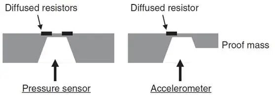
The resistors in piezoresistive sensors—which act as strain sensing elements—are typically mounted on flexible surfaces or structures; microfabrication techniques can be used to selectively remove substrate material, thereby reducing the stiffness of the device’s sensing area. Such sensors are frequently used in the automotive, medical and industrial control sectors.
![图片[1]-一文解读微机电系统的基础知识-大连富泓机械有限公司](/wp-content/uploads/2026/07/1783254614628_0.jpg)
Figure 1: Two types of silicon microsensors fabricated using the piezoresistive effect in semiconductors
Among MEMS sensors, capacitive sensing is widely used due to its simple structure. The capacitance C of the device, defined as the capacitance between its two electrodes, can be calculated using the formula C = (ε₀ × ε_r × A) / d, where ε₀ represents the permittivity of free space, ε_r denotes the relative permittivity of the material between the electrodes, A is the capacitive area, and d is the distance between the electrodes. Capacitive sensors achieve detection primarily through five methods: firstly, by altering the distance between the electrodes; secondly, by changing the position of the central electrode relative to the two outer electrodes to enable differential measurement; thirdly, by altering the area of overlap between the electrodes; fourthly, by altering the differential area of overlap between the electrodes; and fifthly, by altering the position of the dielectric within the space between the electrodes (as illustrated in Figure 2).
![图片[2]-一文解读微机电系统的基础知识-大连富泓机械有限公司](/wp-content/uploads/2026/07/1783254614628_1.jpg)
Figure 2: Different configurations of capacitors used as sensing elements
The piezoelectric effect is a key physical phenomenon in the manufacture of microsensors; it refers to the generation of electric polarisation—that is, an electric potential—within a material in response to mechanical strain, whilst the application of an electric field induces mechanical strain in the material. The former is utilised in sensors, whilst the latter is commonly employed in actuators. Silicon and germanium are crystals with centre symmetry and do not exhibit the piezoelectric effect unless strain is induced; materials lacking centre symmetry, such as quartz, lead zirconate titanate (PZT) and zinc oxide (ZnO), possess piezoelectric properties. Among these, PZT and ZnO can be deposited onto substrates in the form of thin films for use in the manufacture of micro-electromechanical systems (MEMS).
![图片[3]-一文解读微机电系统的基础知识-大连富泓机械有限公司](/wp-content/uploads/2026/07/1783254614628_2.jpg)
Example of the cross-sectional structure of a piezoelectric MEMS loudspeaker
(2) Microactuator technology
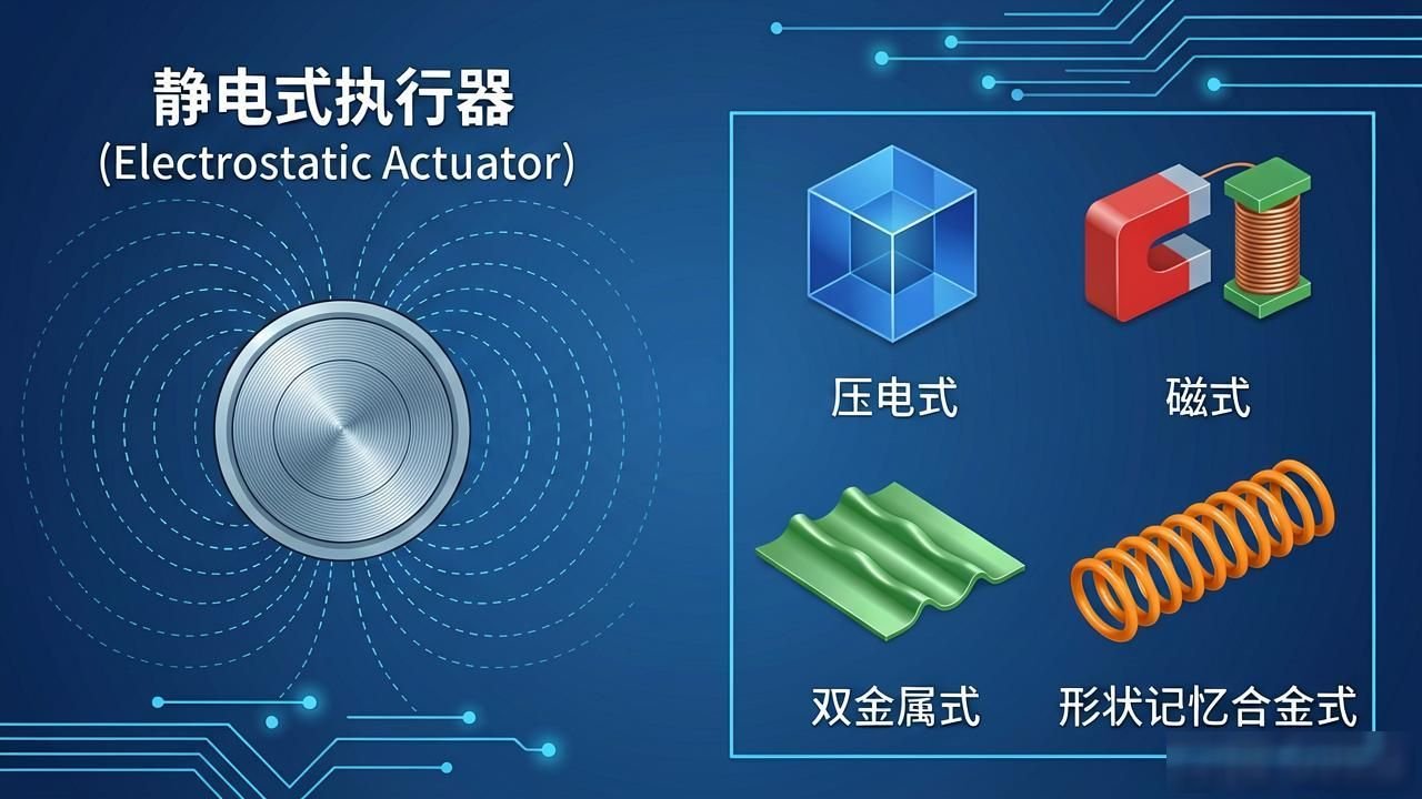
MEMS actuators are realised using a variety of principles, including electrostatic, piezoelectric, magnetic, bimetallic and shape memory alloy (SMA) principles. Each principle has its own characteristics, and the appropriate one must be selected according to the specific application.
Electrostatic actuation utilises the mutual attraction between two plates with opposite charges; when a voltage V is applied, the force F generated between the plates can be calculated using the formula F = (ε₀ × ε_r × A × V²) / (2 × d²), where the parameters have the same meanings as in the capacitance formula. This drive method is easy to manufacture and can be integrated with electronic devices; it has low power consumption and high mechanical bandwidth. However, the force varies non-linearly with displacement and the applied voltage; the force generated is relatively small, and the operating voltage may be relatively high.
Bimetallic microactuators operate by utilising the difference in the coefficients of thermal expansion between two different materials. The composite structure, made from these two materials, generates thermally induced stresses when heated; if the structure possesses sufficient flexibility, it will bend, and its thermal strain can be calculated using the formula.
Perform the calculation, where αfilmA is the coefficient of thermal expansion of the top film, αfilmB is the coefficient of thermal expansion of the bottom film, T is the temperature of the bimetallic element, and T_environment is the ambient temperature.
Actuators of this type are capable of achieving a reasonable displacement, with a linear relationship between deflection and power; however, they have high heating power consumption, low mechanical bandwidth, are relatively complex to design and manufacture, and are sensitive to environmental conditions. By depositing a thin aluminium film onto a thin, flexible silicon cantilever beam and applying an electric current to the aluminium layer to generate Joule heating, it is possible to fabricate a simple bimetallic microactuator; due to the difference in the coefficients of thermal expansion between the two materials, the cantilever beam will bend.
Shape memory alloys (SMAs) are commonly used in the manufacture of microactuators; when heated, they undergo a phase transition from martensite to austenite and return to a strain-free state, thereby exhibiting a memory effect. When used as an actuator, SMA remains in the martensitic phase and is strain-free at room temperature; after a strain is applied at room temperature, heating induces the phase transformation, enabling strain recovery and thereby yielding a high actuator energy density.
SMA can be deposited as a thin film onto silicon wafers using sputtering, typically aided by Joule heating; It exhibits a memory effect, which is reversible and can be reused; it is characterised by high energy density and can achieve a large recovery strain exceeding 81 TP3T. However, it suffers from high power consumption and has a low mechanical bandwidth, its fabrication process is relatively complex, and repeated cycling at high strain levels may lead to fatigue.
(3) Materials commonly used in micro-electro-mechanical systems
Materials used in the manufacture of micro-electro-mechanical system (MEMS) devices include semiconductors, metals, glass, ceramics and polymers, amongst others. MEMS devices must fulfil a wide range of functional requirements, including electrical, mechanical, chemical and thermal requirements. Therefore, when selecting materials, it is necessary to comprehensively consider both their electrical and non-electrical properties.
Silicon is an extremely common material in micro-electro-mechanical systems (MEMS). The relevant infrastructure and body of knowledge are well-established, and it possesses outstanding mechanical properties, with a yield strength approaching that of stainless steel and a strength-to-weight ratio that ranks among the highest of all engineering materials. However, silicon has its limitations: once strain exceeds its limit, catastrophic failure occurs; furthermore, it is anisotropic, meaning that its material properties vary depending on the orientation of the crystal axes relative to the applied load. These factors must all be taken into account during device design.
With regard to thin-film materials, in addition to monocrystalline silicon, materials such as polycrystalline silicon, silicon nitride, deposited glass and aluminium are also widely used in the manufacture of micro-electromechanical systems (MEMS). These thin films are typically deposited using chemical vapour deposition (CVD) processes, such as low-pressure chemical vapour deposition (LPCVD) and plasma-enhanced chemical vapour deposition (PECVD), or through physical vapour deposition (PVD) methods, such as evaporation and sputtering.
Many of the numerous thin-film deposition techniques are cost-effective and are popular choices in microelectronics manufacturing; however, they typically generate significant residual stresses and stress gradients, which pose challenges for the manufacture of micro-electro-mechanical systems (MEMS) devices with mechanical functions. The residual stress and stress gradients in thin films are related to the type of material, deposition temperature, deposition method and substrate material; their values can range from high compressive stress to high tensile stress.
Process conditions and procedures are highly dependent on material properties during the manufacturing process, particularly mechanical properties. Residual stresses present after film deposition may undergo significant changes during subsequent thermal processing steps. Furthermore, as each MEMS device typically involves a bespoke manufacturing process, it is difficult to predict the final stress values of the films in advance, Consequently, the development and manufacture of MEMS devices must be carried out in parallel with the measurement of material properties, utilising iterative design optimisation; this, in turn, leads to increased development time and costs.
Furthermore, there are difficulties in determining the properties of thin-film materials; for example, it is not possible to carry out load–deflection measurements after peeling the film away from the substrate. However, given that a variety of test structures have now been designed in the field of micro-electromechanical systems, these can be used to measure key material properties.
(iv) Design tools for micro-electro-mechanical systems
Compared with integrated circuit design, the design of micro-electro-mechanical systems is more complex. In the field of integrated circuits, manufacturing processes and design rules are relatively well-established; designers integrate these into computer-aided design tools and, by considering only electrical effects, are able to carry out their design work, with the relevant tools providing a high degree of accuracy in predicting device performance.
The design of micro-electro-mechanical systems (MEMS) presents multiple challenges: customised manufacturing processes must be developed for each type of device; design rules remain unknown until the process has been finalised; and material properties depend on as yet unknown manufacturing processes and conditions. many MEMS devices simultaneously exhibit a wide range of physical phenomena—including electrical, mechanical, thermal and chemical phenomena—which in turn give rise to strongly coupled fields; furthermore, MEMS designers must possess in-depth knowledge of manufacturing processes.
Process modelling tools are broadly similar to those used in the integrated circuit industry; they assist designers in creating process models and mask patterns, and utilise numerical techniques to simulate fabrication steps. However, their ability to predict mechanical and material properties is relatively limited; one of their key advantages is the ability to generate three-dimensional renderings of devices.
There are design tools at the physical level that use partial differential equations to model the behaviour of components within a real three-dimensional continuum; these encompass both analytical and numerical tools, such as the finite element method, the boundary element method and the finite difference method, Most of these are refined versions of numerical modelling tools used in macroscopic design; that is the case.
A device-level model is a macro model or a reduced-order model; it is capable of capturing the physical behaviour of a component within a limited scope and is compatible with system-level models. A system-level model is a high-level block diagram and a lumped-parameter model, which describes the system as a set of coupled ordinary differential equations.
Methods for the manufacture of micro-electro-mechanical systems
The manufacture of micro-electro-mechanical systems (MEMS) incorporates established technologies from the field of integrated circuits—such as oxidation, diffusion, ion implantation, low-pressure chemical vapour deposition (LPCVD) and sputtering—whilst also combining specialised micromachining processes. These manufacturing techniques are highly customisable and offer a wide range of processing capabilities.
Micro-electromechanical systems (MEMS) devices, which have a wide range of applications and are widely used, are similar to integrated circuit chips in that both are manufactured using semiconductor technology.
(1) Front-end manufacturing processes
The oldest form of micromachining is volumetric micromachining, in which micro-mechanical components are fabricated by selectively removing substrate material; this can be achieved using chemical, physical or chemomechanical methods, with wet chemical volumetric micromachining being widely used in industry.
One commonly used bulk micromachining technique is chemical wet etching, which involves immersing the substrate in a reactive chemical solution, allowing the exposed areas to be etched at a measurable rate. It offers high etching rates and high selectivity, and the process can be optimised by adjusting parameters such as the composition of the etching solution, temperature, substrate doping concentration and crystal plane orientation. Its fundamental mechanism comprises three steps: reactant transport, surface reaction and product transport. Depending on the rate-limiting step, it is classified as either “diffusion-limited”—where the rate can be increased by stirring—or “reaction-rate-limited”, which offers superior reproducibility and etching rates and is more commonly used in practical applications.
In micro-machining, chemical wet etching is primarily categorised into isotropic wet etching and anisotropic wet etching. The etching rate in isotropic wet etching is largely independent of the crystal orientation of the substrate, etching proceeds uniformly in all directions. The most commonly used etchant for silicon is a mixed solution of nitric acid (HNO₃), hydrofluoric acid (HF) and acetic acid (HC₂H₃O₂); the reaction equation is Si + HNO₃ + HF → + NO + H₂O, This reaction is autocatalytic due to the regeneration of nitrous acid, and must be carried out under vigorous stirring to ensure that the lateral and vertical etching rates are consistent. The masking materials used are typically silicon dioxide and silicon nitride, with silicon nitride being more commonly used due to its lower etching rate.
The orientation of the substrate crystal influences the rate of anisotropic wet etching; there are significant differences in etching rates across different planes of a silicon crystal; these differences are related to the bond configurations and atomic densities of the respective planes. Such etching is generally characterised by comparing the etching rates along the plane, perpendicular to the crystal plane, and normal to the crystal plane, with the etching rate along the plane being the slowest; the difference in etching rates between different crystal orientations can be as high as 1000:1. This is because the density of exposed silicon atoms is highest on the (111) plane, and the three silicon bonds beneath the plane form a chemical shield.
Thanks to this characteristic, anisotropic wet etching enables high-resolution etching and strict dimensional control, and allows for double-sided processing to form self-isolated structures, which is beneficial for the packaging of micro-electromechanical system (MEMS) devices—such as pressure sensors—exposed to harsh environments. It is currently widely used in the manufacture of devices such as silicon pressure sensors and bulk micromachined accelerometers, and the technology has been well-established for 30 years.
Oriented silicon substrates, following anisotropic wet etching, can form inverted pyramid-shaped etched pits, as well as flat-bottomed trapezoidal etched pits (as shown in Figure 3), Scanning electron microscope (SEM) images clearly reveal the trapezoidal etched pits and show the back-side structure of the thin film used in pressure sensors (as shown in Figures 4a and 4b).
![图片[5]-一文解读微机电系统的基础知识-大连富泓机械有限公司](/wp-content/uploads/2026/07/1783254614628_5.png)
Figure 3: A schematic illustration showing an oriented silicon substrate immersed in a solution of anisotropic wet etchant, subsequently taking on the shape of the etched profile.
![图片[6]-一文解读微机电系统的基础知识-大连富泓机械有限公司](/wp-content/uploads/2026/07/1783254614628_6.jpg)
These are Figures 4(a) and 4(b), respectively, which show SEM images of an oriented silicon substrate immersed in an anisotropic wet etchant; the scale bar is 1 micrometre.
Commonly used wet etching agents with anisotropic properties broadly fall into three categories. The first comprises aqueous alkaline solutions, such as potassium hydroxide (KOH), ammonium hydroxide (NH₄OH) and tetramethylammonium hydroxide (TMAH), amongst others. These etchants exhibit high etching rates, and the ratio of planar etching rate to non-planar etching rate is relatively high; however, under specific conditions, TMAH exhibits an extremely low etching rate for aluminium, making it suitable for pre-treated microelectronic wafers; however, its etching rate for silicon dioxide masks is relatively high, which may lead to alkali contamination of the wafer—though this can be mitigated by appropriate cleaning procedures; Secondly, ethylenediamine and hydroquinone, known as EDP, have an even higher ratio of vertical to planar etching rates and are compatible with a wider range of mask materials; however, they are carcinogenic, the etching process is difficult to monitor, and cleaning presents challenges; thirdly, there are other specialised etching agents.
Silicon nitride is a commonly used mask material for anisotropic wet etching; thermally grown silicon dioxide can also be used, although care must be taken to control the thickness, particularly when using KOH as the etchant. Photoresist cannot be used with any anisotropic etchant. Metals such as tantalum (Ta) and gold (Au) exhibit good etch resistance in EDP; aluminium also exhibits etch resistance to TMAH under specific conditions.
Etching rate, etching rate ratio and etching selectivity—which are characteristics of anisotropic etchants—depend primarily on the chemical composition of the solution and temperature, and follow the Arrhenius equation: R = R₀ exp(−E_a/(κT)), where R₀ denotes a constant, E_a represents the activation energy, k is the Boltzmann constant, and T is the temperature in kelvins.
In micro-machining, precise control of silicon film thickness or etching depth is a key requirement; however, due to factors such as load effects, temperature variations and differences in substrate thickness, it is difficult to ensure etching uniformity. Time-controlled etching determines depth based on the product of etching rate and time; however, it is difficult to control and is susceptible to a variety of factors. Consequently, etch-stop methods have been developed, which primarily include doped etch-stop and electrochemical etch-stop methods.
An etch-stop layer is formed by high-concentration p-type boron doping, i.e. greater than 5×10¹⁹ cm⁻³, this process is known as the doped etch-stop method, which significantly reduces the etch rate in highly doped regions, as illustrated in Figure 5; however, the problem is that a highly doped surface layer may not be suitable for certain devices, such as piezoresistive devices; The electrochemical etch-stop method offers good dimensional control and can also produce lightly doped material films suitable for high-quality piezoresistive devices; however, it requires specialised fixtures and electronic control systems.
![图片[8]-一文解读微机电系统的基础知识-大连富泓机械有限公司](/wp-content/uploads/2026/07/1783254614628_8.jpg)
Figure 5 shows the relationship between the etching rate of oriented silicon wafers and boron concentration under different etchant concentrations.
Surface micromachining is a mainstream manufacturing technique; its core process involves depositing a thin-film material to serve as a temporary sacrificial layer, depositing and patterning a structural layer—that is, the thin-film device layer—on top of the sacrificial layer, and then removing the temporary sacrificial layer, thereby releasing the mechanical structural layer from its constraints and allowing it to move freely. Taking the fabrication of a polycrystalline silicon cantilever beam as an example, an oxide sacrificial layer is first deposited and patterned, followed by the deposition and patterning of the polycrystalline silicon structural layer; finally, removal of the sacrificial layer yields a freely movable cantilever beam, as shown in Figure 6.
![图片[9]-一文解读微机电系统的基础知识-大连富泓机械有限公司](/wp-content/uploads/2026/07/1783254614628_9.jpg)
Figure 6: Schematic diagram of the surface micromachining process
This technology allows for precise control of vertical dimensions, which are determined by the thickness of the deposited film; horizontal dimensions can also be precisely controlled, with these being determined by the fidelity of the photolithography and etching processes. It is compatible with microelectronic devices, thereby enabling integration. Furthermore, by utilising the characteristics of thin-film deposition—such as the conformal coverage offered by LPCVD—and employing a single-sided wafer processing method, it achieves a higher integration density than other methods, whilst the cost per chip is lower than that of other approaches.
The drawback is that the mechanical properties of the structural film are unknown, which necessitates measurement; furthermore, the residual stress is high and must be reduced through high-temperature annealing; Residual stress also varies with subsequent thermal processing, making it difficult to achieve reproducibility of mechanical properties; furthermore, during the release of the structural layer, adhesion is likely to occur due to capillary forces, necessitating specialised release processes and anti-adhesion coatings. Figure 7 illustrates the structure of a polycrystalline silicon resonator fabricated using surface micromachining techniques.
![图片[10]-一文解读微机电系统的基础知识-大连富泓机械有限公司](/wp-content/uploads/2026/07/1783254614628_10.jpg)
Figure 7: Structure of a polycrystalline silicon resonator fabricated using surface micromachining techniques
The technology used to join two or more wafers together to form a multi-wafer stack is known as wafer bonding. It is primarily divided into three categories: direct bonding (also known as fusion bonding), field-assisted bonding (also known as anodic bonding), and bonding using an intermediate layer. All these methods require the substrates to possess high flatness, as well as smoothness and cleanliness.
Direct bonding is commonly used to join silicon wafers to one another, or to bond silicon to silicon oxide wafers. The basic process comprises five steps: cleaning and surface preparation, pre-bonding, pre-annealing inspection, high-temperature annealing (generally at around 1000°C), and final inspection. The wafers are initially bonded via hydrogen bonds formed by surface hydration; following high-temperature annealing, the bond strength is comparable to that of monocrystalline silicon, whilst plasma treatment can reduce the annealing temperature to 250–300°C or even lower.
Anode bonding, which bonds silicon wafers to Pyrex 7740 wafers, is achieved using an electric field and high temperatures. A strong electric field is formed through the migration of sodium ions within the Pyrex glass, thereby enabling surface chemical fusion. It offers the following advantages: Pyrex 7740 has a coefficient of thermal expansion similar to that of silicon and exhibits very low residual stress; consequently, it is widely used in the packaging of micro-electromechanical systems (MEMS).
In addition, eutectic bonding—that is, the bonding method using a gold interlayer—and glass paste bonding, which is achieved using a glass paste interlayer, and polymer bonding, which utilises interlayers such as epoxy resin and polyimide; each of these methods has its own specific applications in the manufacture of micro-electromechanical systems (MEMS).
Micro-electromechanical systems (MEMS) fabrication technologies capable of producing microstructures with extremely deep features and high aspect ratios include deep reactive ion etching (DRIE) of silicon; deep reactive ion etching of glass; LIGA technology; and thermal imprinting. DRIE of silicon is a highly anisotropic plasma etching process, with etching depths ranging from tens of micrometres to hundreds of micrometres, and is even capable of penetrating the silicon substrate. The mainstream process is the Bosch process, This process alternates between sulphur hexafluoride (SF₆) etching cycles and octafluorocyclobutane (OCB₈) polymer deposition cycles to achieve deep trench fabrication (as shown in Figure 8).
![图片[11]-一文解读微机电系统的基础知识-大连富泓机械有限公司](/wp-content/uploads/2026/07/1783254614628_11.jpg)
Figure 8: Schematic diagram illustrating the principle of deep reactive ion etching (DRIE)
The sidewalls formed on the material during this etching process exhibit a morphology that is both corrugated and scallop-like. The latest equipment of this kind is now capable of achieving etching rates exceeding twenty micrometres per minute, with a mask selectivity of seventy-five to one when etching photoresist, and 150:1 when etching oxides, and the aspect ratio is also exceptionally good, reaching up to 30:1, with 15:1 being the most commonly used ratio in practice. The silicon microstructures fabricated using this process are clearly illustrated in cross-sectional SEM images, which distinctly demonstrate the high aspect ratio and deep trench characteristics, as shown in Figure 9.
![图片[12]-一文解读微机电系统的基础知识-大连富泓机械有限公司](/wp-content/uploads/2026/07/1783254614628_12.jpg)
Figure 9 shows a photograph of a cross-section of a silicon wafer, taken using a scanning electron microscope (SEM); it illustrates the high aspect ratio and deep trench structures that can be fabricated using deep reactive ion etching (DRIE) technology.
In certain circumstances, deep reactive ion etching of glass can form grooves with depths exceeding 100 micrometres and aspect ratios greater than 4:1, as illustrated in Figure 4.10. This process utilises a nickel hard mask, with a selectivity ratio of approximately 10:1. The etching process is characterised by continuous, scallop-free patterns; however, it is susceptible to the influence of the micromask. There is also the LIGA (Liquid-In-Glass-Assisted Etching) technique, which first involves X-ray exposure of a PMMA layer, followed by development and metal deposition, after which the PMMA is removed to yield the metal microstructure. This technique offers advantages such as smooth sidewalls, good verticality and deep penetration; however, it is relatively costly, although variants can reduce costs through the reuse of tool inserts. Hot stamping technology utilises metal tool inserts to transfer patterns onto a polymer substrate through a stamping process. It is characterised by low cost and good dimensional control, making it suitable for the production of microfluidic components.
![图片[13]-一文解读微机电系统的基础知识-大连富泓机械有限公司](/wp-content/uploads/2026/07/1783254614628_13.jpg)
Figure 10 is a scanning electron microscope (SEM) image showing a structure with a high aspect ratio etched into a glass substrate. The image was produced by the Micro-Electro-Mechanical Systems and Nanotechnology Exchange Centre.
(2) Other micro-machining technologies
Furthermore, in addition to the core processes mentioned above, xenon difluoride (XeF₂) dry etching technology, electrical discharge micro-machining (EDM), laser micro-machining, and focused ion beam (FIB) micro-machining, among others, all play a significant role in the manufacture of micro-electro-mechanical systems (MEMS).
XeF₂ dry etching is an isotropic etchant for silicon; it offers high selectivity for materials such as silicon nitride and silicon dioxide, presents no adhesion issues, and is suitable for microstructure fabrication on CMOS wafers; Electrical discharge micro-machining utilises electrical breakdown discharge to remove conductive materials; it is capable of producing micropores measuring tens of micrometres, but as it is a serial process, it is slow and costly; Laser micromachining utilises focused laser energy to melt, vaporise or photodissolve materials; it is suitable for a wide range of materials, and the application of femtosecond laser technology has further improved processing precision and material compatibility; FIB microfabrication can focus the spot size to 50 nanometres, enabling the fabrication of extremely small structures; it can also perform a variety of tasks such as ion-induced deposition, photolithography and doping, and is equipped with imaging and compositional analysis capabilities.
Future Trends in Micro-Electro-Mechanical Systems
Micro-electro-mechanical systems (MEMS) will continue to evolve towards higher levels of integration, greater functionality and smaller dimensions. As manufacturing capabilities improve, it is expected that multiple sensors, various actuators and advanced electronic devices will be integrated onto a single silicon wafer, achieving multifunctionality within a very small space whilst maintaining low costs. At the same time, the deep integration of MEMS and nanotechnology will continue to intensify, driving the further expansion of performance boundaries and broadening the scope of potential applications.
The Internet of Things (IoT), which utilises communication networks to connect physical objects, thereby enabling the collection, storage, processing and exchange of information, has its core development focus on the application of micro-electro-mechanical systems (MEMS). MEMS devices are capable of meeting the IoT’s demand for low-cost, unobtrusive devices that combine sensing and control capabilities. They will play a significant role in numerous fields, including smart homes, the Industrial Internet of Things, intelligent transport and healthcare, and will become a key driver of the IoT’s expansion.
reach a verdict
Micro-electro-mechanical systems (MEMS) technology is a multidisciplinary field that integrates knowledge from various disciplines; it is a comprehensive technology with diverse fabrication capabilities. It is neither a single manufacturing process tailored to a specific application nor one designed for a particular device. By utilising miniaturisation, it transforms the design philosophy of mechanical systems; through mass production, it changes the design philosophy through mass production, and it transforms the design philosophy of mechanical systems through integration with electronic devices, thereby providing new capabilities for the development of smart products across various fields.
Although MEMS devices generally account for only a small proportion of a product’s cost, size and weight, they play a crucial role in the product’s performance, reliability and affordability. The MEMS industry shares common origins with the integrated circuit industry; however, it has a broader range of applications and a greater diversity of technological forms, it has evolved into an independent, landmark technology. In the era of the Internet of Things, the diversity, economic significance and potential scope of application of MEMS will continue to expand, providing support for scientific and technological progress and industrial upgrading.



 Chinese
  Japanese
  English
  German
  Finnish
No comments